Manufacturing
Specialized PCB Manufacturing CompanyProcess
01
Cutting
Process of Cutting raw materials into in-house work dimensions according to product specifications;
02
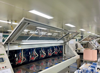
Inner Layer Circuit Formation
Attach a dry film to the surface of the raw material with heat and pressure, then examine the light using the film and
DATA, and form a circuit through a phenomenon.After circuit formation, conduct AOI inspection to automatically check for minor defects or faulty parts of the product.
03
Stacking
Stacking the inner layer substrate where the circuit is made, Prepreg, and the outer layer copper foil to maintain
alignment according to design specifications;
04
Drill
Process of machining holes on the Working Panel using CNC method with in-house edited X-Y Coordinates based on
customer's HOLE information
05
Copper Plating
Process of plating the wall inside a hole with a conductive material (copper) to enable electrical connection without conductivity;
06
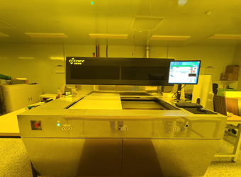
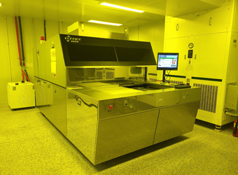
Outer Layer Circuit (LDI)
Attach the dry film to the surface of the raw material with heat and pressure, then examine the light using film & DATA,
and form a circuit through a phenomenon.After circuit formation, conduct AOI inspection using a high-resolution camera to automatically check for minor defects
or faulty parts of the product.
07
PSR
Coating of an invariant ink, an enduring compound under a physical and chemical environment, on a plated copper foil circuit to protect the circuit and prevent SOLDER BRIDGE phenomenon between circuits.(PSR front - PSR printing - PSR exposure - PSR phenomenon)
08
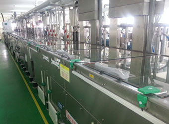
Surface treatment
OSP, HASL, and gold plating are processes to prevent oxidation and contamination of substrate surfaces and to enhance parts assembly.
- OSP: A process that chemical rust inhibitor reacts only with copper elements such as Through Hole, Land, etc., to form a thin, uniform protective membrane of about 0.2-0.5 microns.
- HASL: Immersing a high-temperature, solder-melting TANK substrate and blowing it with high-temperature, high-pressure air to apply solder lead uniformly to uncoated areas.
- Gold plating: A process of nickel and gold plating by electrical precipitation.
Plating is selectively performed only for the CONTACT FINGER AREA based on customer requirements in areas where electrical characteristics are needed.
09
External processing
The process of shaping the WORKING PANEL used to enhance productivity into the final product size and shape requested by the customer.
The process involves using CNC ROUTER M/C, ROUTER BIT, and PROGRAM DATA. (Mold processing - routing - V-Cutting)
10
BBT
After the completion of PCB processing, the process of testing basic electrical performance such as electrical defects on circuits,
open & short, insulation interval violations, etc. with a multi-tester.A TEST FIXTURE (JIG) should be prepared separately, and the types of TEST equipment include DEDICATED and UNIVERSAL.
11
Inspection
The process of inspecting the circuit connection status and appearance of the manufactured PCB is divided into visual inspection
and automatic equipment inspection.
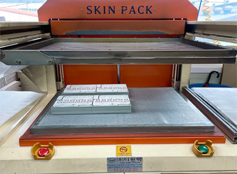
12
Packaging
The process of packaging products individually and in units for delivery to customers.
After vacuum packaging, they are packed again with a buffer and, upon customer request,
BOX label is applied, and a shipment inspection report is attached.